ZnO Thin Film Transistors for Flexible Electronics
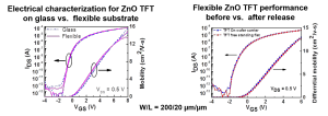
Low-temperature PEALD process allows to build ZnO TFTs directly on ~5-mm think flexible polymeric film, which is initially spin-coated on rigid substrate. The device performance is very similar to that on glass substrate. Also, it is typically unchanged after mechanical peeling with the mobility of > 12 cm2/V-s. Using a home-built bending tester, the flexibility and stability of flexible ZnO TFTs is studied under repeated bending cycles with in-situ electrical measurement.
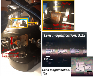
Flexible Electronics Bending Test Tool Design
- Microscopic defects can be observed and video-recorded during bending cycles
- Device is bent along the roller as the belt is moving back and forth
- Kapton belt is used to avoid direct contact between device and the roller
Bending cycles can also be performed on TFTs made from two-dimensional transition metal dichalcogenides. Read more here…
ZnO Thin Film Transistors for Biosensing Applications (in collaboration with Dr. Esther Winter Gomez)
Lipid membrane functionalized ZnO thin film transistors (TFTs) provide a platform for robust and label-free sensing of interactions at membrane surfaces. This can enable membrane biology studies and medical diagnostics of water-borne diseases. Ultra-thin ZnO TFT structures are easily tailorable, provide great flexibility in device layout and can be prepared on polymeric substrates providing flexibility in biosensor design with low fabrication cost.
Fabrication of enclosed PMGI microfluidic channels for ZnO TFTs ensures precise coverage of lipid membrane assemblies on the transistor devices
Fluorescence microscopy imaging can be done to ensure uniform coverage of lipid membranes over ZnO TFTs. Lipid membrane functionalized TFTs have a different surface charge distribution than bare TFTs and show a shift in turn-on voltage during electrical characterization
Integration with Thin Film Pb[ZrxTi1-x]O3 (PZT) on Flexible Polymer Substrates (in collaboration with Dr. Susan Trolier- Mckinstry)
Thin Film PZT Transfer from Silicon onto Polyimide
By etching away a ZnO sacrificial layer, we obtain PZT on solution-cast polyimide
- Enhanced remanent polarization
- Higher permittivity at low frequencies
- Made film stacking possible using Au/In transient liquid phase bonding
- Released PZT on polyimide exhibits larger (10x) reduction in permittivity after poling
- More ferroelastic domain wall switching.
- A lower value in relative permittivity is favorable for energy harvesting purpose (Figure of Merit = e_(31,f)^2∕ε_r “)”.
Thin-Film PZT Stacking Au-In TLP Bond
High Voltage Thin Film Transistor (HVTFT)
PZT actuator array: piezoelectric capacitor are biased to tune the position of array of mirrors, ZnO TFTs are used to as the switch for each pixel. Larger breakdown voltage means larger operation range for the PZT capacitor.
Offset-Drain PEALD ZnO Thin Film Transistors
The introduction of drain offset structure affects the device performance in linear region (left). In saturation region (right) little reduction of µFE is found.
Breakdown
Breakdown voltage increases linearly with drain offset size and it is not affected by source offset. Further increase in Vds causes dielectric breakdown followed by burnout at the drain offset region.
Transition Metal Dichalcogenide (TMD) Dry Etch Process
- Etch rate of WS2 and MoS2 show plasma power dependent etching rate.
- The difference in etching rate may be related to the larger sputter yield of Mo compared to W, leading to larger etch rates for MoS2
- WS2 measurements at low plasma power were under RIE for 2 min run and a 3 min run respectively.
- Optimization of thinning process can give rise to improvement in TMD transistor with reproducible results


