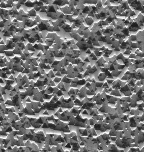
Two dimensional (2D) materials consist of ultra-thin sheets of atoms that exhibit remarkably different properties from their 3D bulk counterparts. Examples include graphene and the layered chalcogenide family of materials which includes compounds such as the transition metal dichalcogenides (MoS2, WSe2, etc.), the group IV chalcogenides (SnS2, SnS, SnSe2),and the bismides (Bi2Se3, Bi2Te3). Layered chalcogenides crystallize into covalently bonded sheets of atoms that are held together via van der Waals forces. This class of 2D materials exhibits a remarkable range of electronic properties with thickness-dependent bandgap energies that span the range from ~0.3 to 2.0 eV. Consequently, there is significant interest in monolayer and few layer films of layered chalcogenides for potential applications in optoelectronics, sensing, thin film transistors and flexible electronics.
Our research is focused on the development of epitaxial growth techniques to deposit monolayer and few layer films of layered chalcogenides such as WSe2 and WS2. Current studies focus on investigating the impact of the substrate, growth chemistry and processing conditions on nucleation and growth of monolayer and few layer films and characterizing the electrical and optical properties of the layers.