
Defect Engineering of Two-Dimensional Transition Metal Dichalcogenides
Z. Lin, B. R. Carvalho, E. Kahn, R. Lv, R. Rao, H. Terrones, M. A. Pimenta, M. Terrones. (2016). “Defect engineering of two-dimensional transition metal dichalcogenides“. 2D Materials 3, 022002.
“Two-dimensional transition metal dichalcogenides (TMDs), an emerging family of layered materials, have provided researchers a fertile ground for harvesting fundamental science and emergent applications. TMDs can contain a number of different structural defects in their crystal lattices which significantly alter their physico-chemical properties. Having structural defects can be either detrimental or beneficial, depending on the targeted application. Therefore, a comprehensive understanding of structural defects is required. Here we review different defects in semiconducting TMDs by summarizing: (i) the dimensionalities and atomic structures of defects; (ii) the pathways to generating structural defects during and after synthesis and, (iii) the effects of having defects on the physico-chemical properties and applications of TMDs. Thus far, significant progress has been made, although we are probably still witnessing the tip of the iceberg. A better understanding and control of defects is important in order to move forward the field of Defect Engineering in TMDs. Finally, we also provide our perspective on the challenges and opportunities in this emerging field.”
The Role of Defects and Doping in 2D Graphene Sheets and 1D Nanoribbons
H. Terrones, R. Lv, M. Terrones, M. S. Dresselhaus. (2012). “The role of defects and doping in 2D graphene sheets and 1D nanoribbons“. Reports on Progress in Physics 75, 062501.
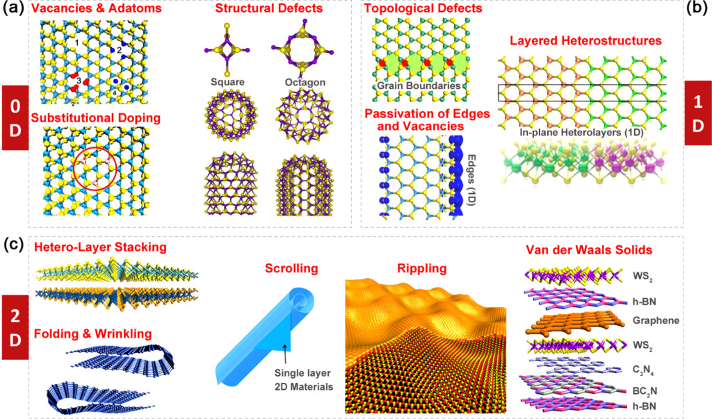
“Defects are usually seen as imperfections in materials that could significantly degrade their performance. However, at the nanoscale, defects could be extremely useful since they could be exploited to generate novel, innovative and useful materials and devices. Graphene and graphene nanoribbons are no exception. This review therefore tries to categorize defects, emphasize their importance, introduce the common routes to study and identify them and to propose new ways to construct novel devices based on ‘defective’ graphene-like materials. In particular, we will discuss defects in graphene-like systems including (a) structural (sp2-like) defects, (b) topological (sp2-like) defects, (c) doping or functionalization (sp2– and sp3-like) defects and (d) vacancies/edge type defects (non-sp2-like). It will be demonstrated that defects play a key role in graphene physicochemical properties and could even be critical to generate biocompatible materials. There are numerous challenges in this emerging field, and we intend to provide a stimulating account which could trigger new science and technological developments based on defective graphene-like materials that could be introduced into other atomic layered materials, such as BN, MoS2 and WS2, not discussed in this review.”

Graphene and Graphite Nanoribbons: Morphology, Properties, Synthesis, Defects and Applications
M. Terrones, A. R. Botello-Méndez, J. Campos-Delgado, F. López-Urías, Y. I. Vega-Cantú, F. J. Rodríguez-Macías, A. L. Elías, E. Muñoz-Sandoval, A. G. Cano-Márquez, J.-C. Charlier. (2010). “Graphene and graphite nanoribbons: Morphology, properties, synthesis, defects and applications“. Nano Today 5, 351-372.
“Carbon is a unique and very versatile element which is capable of forming different architectures at the nanoscale. Over the last 20 years, new members of the carbon nanostructure family arose, and more are coming. This review provides a brief overview on carbon nanostructures ranging from C60 to graphene, passing through carbon nanotubes. It provides the reader with important definitions in carbon nanoscience and concentrates on novel one- and two-dimensional layered carbon (sp2 hybridized), including graphene and nanoribbons. This account presents the latest advances in their synthesis and characterization, and discusses new perspectives of tailoring their electronic, chemical, mechanical and magnetic properties based on defect control engineering. It is foreseen that some of the structures discussed in the review will have important applications in areas related to electronics, spintronics, composites, medicine and many others.”
Electron and Phonon Renormalization Near Charged Defects in Carbon Nanotubes
I. O. Maciel, N. Anderson, M. A. Pimenta, A. Hartschuh, H. Qian, M. Terrones, H. Terrones, J. Campos-Delgado, A. M. Rao, L. Novotny, A. Jorio. (2008). “Electron and phonon renormalization near charged defects in carbon nanotubes“. Nature Materials 7, 878-883.
“Owing to their influence on electrons and phonons, defects can significantly alter electrical conductance, and optical, mechanical and thermal properties of a material. Thus, understanding and control of defects, including dopants in low-dimensional systems, hold great promise for engineered materials and nanoscale devices. Here, we characterize experimentally the effects of a single defect on electrons and phonons in single-wall carbon nanotubes. The effects demonstrated here are unusual in that they are not caused by defect-induced symmetry breaking. Electrons and phonons are strongly coupled in sp2 carbon systems, and a defect causes renormalization of electron and phonon energies. We find that near a negatively charged defect, the electron velocity is increased, which in turn influences lattice vibrations locally. Combining measurements on nanotube ensembles and on single nanotubes, we capture the relation between atomic response and the readily accessible macroscopic behaviour.”
