by Vishal Jindal
1. Abstract
This post calculates the band structure and density of state for an isolated polythiophene chain using density functional theory (DFT) and compares the various electronic properties such as bandgap (Eg), bandwidth and effective charge mass of the valence and conduction bands for different exchange-correlation functionals.
2. Introduction
Polythiophene (PT) is an organic polymer which has the simplest structure among a general class of polymerized thiophenes known as polythiophenes (PTs). In the presence of electron-acceptor materials PTs become conductive and demonstrate interesting optical properties resulting from their conjugated backbone which have made them standard materials for organic semiconductor devices [1,2]. The development of polythiophenes and related conductive organic polymers was recognized by the awarding of the 2000 Nobel Prize in Chemistry to Alan J. Heeger, Alan MacDiarmid, and Hideki Shirakawa “for the discovery and development of conductive polymers” [3]. Electronic transport properties, and optical properties such as light absorption and emission, are dictated by the valence and conduction bands, which are the closest bands to the Fermi level, and the gap between them. The undistorted PT chain has a 1-D semiconductor band structure [4] and the reported experimental value for bandgap is 2.0eV [8].
3. Methodology
We used a plane-wave basis set with ultrasoft pseudopotentials as implemented in the CASTEP code [5] to perform DFT calculations to get band structure and density of states for different exchange-correlation functionals such as LDA CA-PZ, GGA-PBE, GGA-PW91, and GGA-BLYP. Materials Studio was used as a builder, visualizer, and user interface for the CASTEP calculations.

Fig 1. All-trans polythiophene chain with two rings in each unit cell having dimensions 8 x 15 x 15 (in angstroms), here two periodic unit cells are shown.
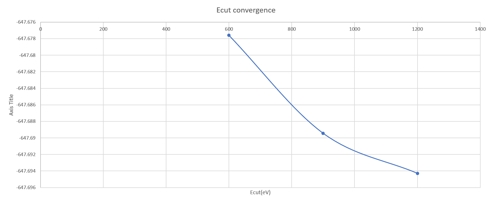
First, the structure of the PT chain was optimized using the Perdew, Burke, and Ernzerhof (PBE) [6] functional described within the generalized gradient approximation (GGA) [7] and the same optimized structure was used to get band structure using different functionals. Based on the work by Joel et al [4], a basis set cutoff energy of 450 eV and k-point sampling of 16 x 1 x 1 (instead of 7 x 1 x 1 used in the paper to increase the k-point sampling) were used. SCF tolerance is taken to be 2.0e-6 eV/atom for all the calculations. The “on the fly” generated ultrasoft pseudopotential for H has a core radius of 0.6 Bohr (~0.32 Å), 1.4 Bohr (~0.74 Å) for carbon (C) and 1.8 Bohr (~0.95 Å) for sulfur (S) and was generated with 4 valence electrons (2s2 2p2) for C and 6 valence electrons (3s2 3p4) for S.
While calculating the band structures, an approximate separation of 0.005 1/Å between k-points was used for each of the different exchange-correlation functionals.
4. Results
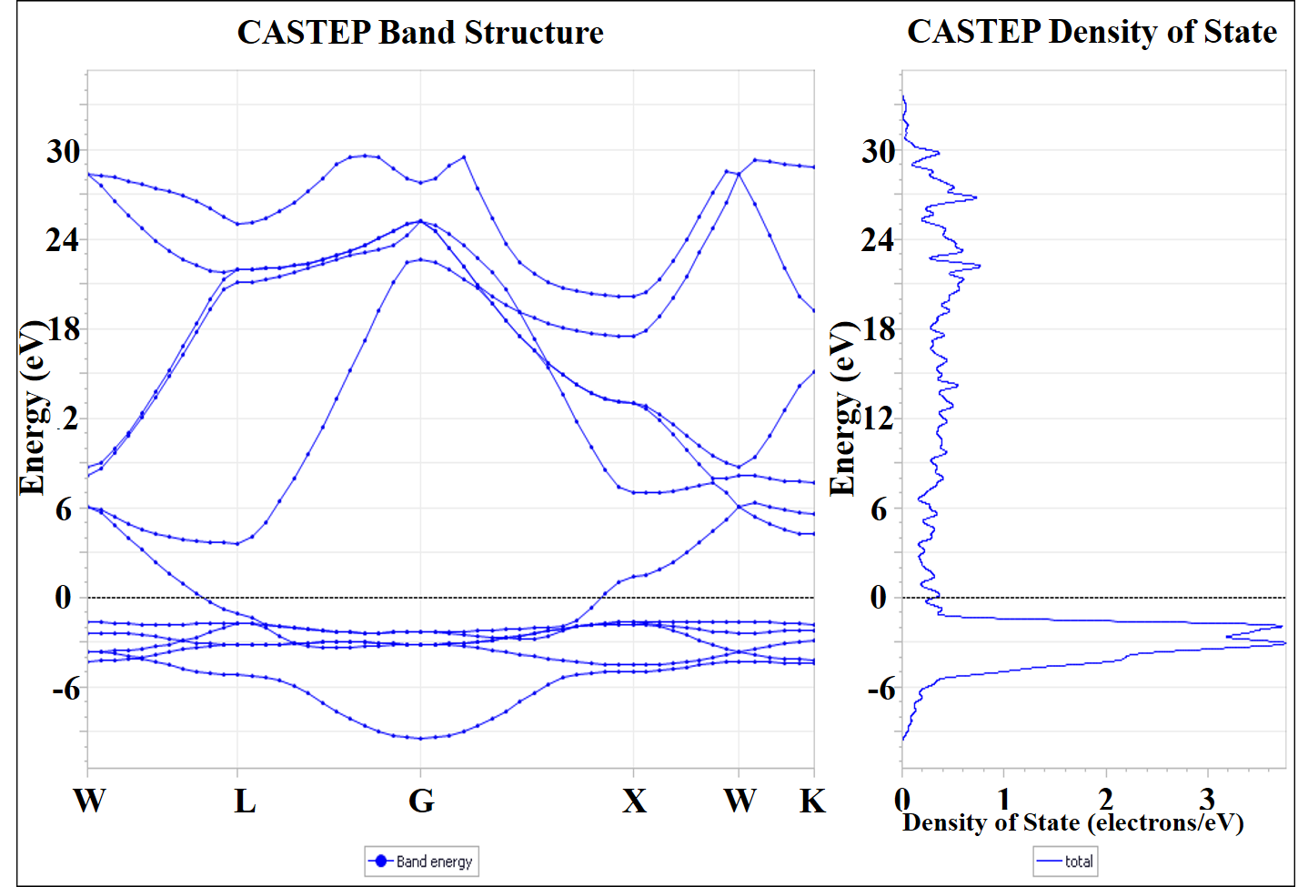
Band Structure


Fig 2. Band structures for polythiophene using LDA, GGA-PBE, GGA-PW91 and GGA-BLYP functionals.
Density of State


Fig 3. The density of state plot for different XC functionals
The band structures and density of states for polythiophene using 4 different exchange-correlation functionals are given in Fig 1. and Fig 2., respectively. The energy band gaps, bandwidth and effective charge mass for valence and conduction bands are calculated for each exchange-correlation functional (XC).
The energy between the valence and conduction band of a polymer is related to the lowest energy of its monomer units and to the bandwidth resulting from the overlap between the
monomer orbitals [9]. A bandgap (𝐸g) is defined as the difference between the highest occupied molecular orbital (HOMO) and the lowest unoccupied molecular orbital (LUMO) energy levels in the polymer [10]: 𝐸g = 𝐸(LUMO) − 𝐸(HOMO) (eV).
In accordance with the band-like theory, the bandwidth (BW) and electron effective
mass (m*) are good parameters for predicting the hole and electron-transporting ability of polymers [11]. Valence (conduction) bandwidth is defined as the energy difference between the first band located right below (above) the Fermi level at Γ-point (k=0) to the M-point (k=1) [12].
The effective mass (m*) of the carrier at the band edge representing mobility was
obtained as the square of ħ (= h/2π) multiplied by the reciprocal of the curvature from E(k) with k (wave vector), and the formulation is defined as:

The denominator of the above equation is calculated by fitting a parabola (y = kx2 + c) using the first 5 data points (which lie between k = 0 to 0.33) of energy vs k plot (band structure) for both conduction and valence for each of the different functional used.
Table 1. (below) shows the bandgap, bandwidths, and effective charge mass calculated using different exchange-correlation (XC) functionals.
| Correlation functional (XC) | Band gap (eV) | Valence band effective mass (-m*) | Valence bandwidth (eV) | Conduction band effective mass (m*) | Conduction bandwidth (eV) |
| LDA CA-PZ | 1.47 | 1.23 | 1.73 | 1.46 | 1.39 |
| GGA PBE | 1.49 | 1.25 | 1.72 | 1.47 | 1.39 |
| GGA PW91 | 1.46 | 1.25 | 1.72 | 1.49 | 1.38 |
| GGA BLYP | 1.46 | 1.25 | 1.72 | 1.49 | 1.38 |
As evident from the results in the table, values of the energy bandgap, valence and conduction bandwidths, and effective masses for carrier charge in valence and conduction bands are approximately the same whether we use the LDA or GGA exchange-correlation functionals for the DFT calculation of band structure.
5. Conclusion
Local density (LDA) and generalized gradient approximation (GGA) density functionals generally underestimate band gaps for semiconductors by about 40% of the actual value [13, 14], but can be valuable to study the shape of the valence and conduction bands. Hybrid functionals such as B3PW91 and B3LYP are known to be better predict the experimental band gaps for semiconductors and insulators [14]. The experimental value of the bandgap for polythiophene was found to be 2.0 eV, which indeed agrees well with the calculated bandgap in the framework of the hybrid (B3LYP) as shown by Kaloni et al. [12].
CASTEP code as implemented using Material Studio, for the calculation of properties such as band structure, does not allow for use of hybrid functionals along with the ultrasoft pseudopotential. Comparing the above results for bandwidths and effective mass using LDA, GGA functionals with the results from using hybrid functionals for our calculations can strengthen the argument that less computationally intensive calculations (involving LDA, GGA functionals) can be used reliably for studying the band properties other than the energy bandgap.
6. References
[1] G. Li, R. Zhu, and Y. Yang, Nat. Photonics, 2012, 6, 153–161.
[2] S. P. Rittmeyer and A. Groß, Beilstein J. Nanotechnol., 2012, 3, 909–919.
[3] https://en.wikipedia.org/wiki/Polythiophene
[4] Joel H. Bombile, Michael J. Janik and Scott T. Milner, Tight binding model of conformational disorder effects on the optical absorption spectrum of polythiophenes, Phys. Chem. Chem. Phys., 2016, 18, 12521.
[5] J. Clark Stewart, D. Segall Matthew, J. Pickard Chris, J. Hasnip Phil, I.J. Probert Matt, K. Refson, C. Payne Mike, First-principles methods using CASTEP, Zeitschrift für Kristallographie – Crystalline Materials, 220(5-6) pp. 567-570 (2005).
[6] J.P. Perdew, K. Burke, M. Ernzerhof, Generalized gradient approximation made simple, Phys. Rev. Lett., 77 (1996) 3865-3868.
[7] J.P. Perdew, J.A. Chevary, S.H. Vosko, K.A. Jackson, M.R. Pederson, D.J. Singh, C. Fiolhais, “Atoms, Molecules, Solids, And Surfaces – Applications of the Generalized Gradient Approximation for Exchange and Correlation,” Phys. Rev. B, 46 (1992) 6671-6687.
[8] Kobayashi M, Chen J, Chung T-C, Moraes F, Heeger A J, Wudl F. Synth Met. 1984;9:77–86. doi: 10.1016/0379-6779(84)90044-4.
[9] U. Salzner, J. B. Lagowski, P. G. Pickup, and R. A. Poirier, Design of low band gap polymers employing density functional theory—hybrid functionals ameliorate band gap problem, Journal of Computational Chemistry, vol. 18, no. 15, pp. 1943–1953, 1997.
[10] E. Bundgaard and F. C. Krebs, Low band gap polymers for organic photovoltaics, Solar Energy Materials and Solar Cells, vol. 91, no. 11, pp. 954–985, 2007.
[11] X.-H. Xie, W. Shen, R.-X. He, and M. Li, A Density Functional Study of Furofuran Polymers as Potential Materials for Polymer Solar Cells, Bulletin of the Korean Chemical Society, vol. 34, no. 10, pp. 2995–3004, Oct. 2013.
[12] Thaneshwor P. Kaloni, Georg Schreckenbach, and Michael S. Freund, Band gap modulation in polythiophene and polypyrrole-based systems, Sci. Rep. 6, 36554; doi: 10.1038/srep36554 (2016).
[13] J. P. Perdew, Density functional theory and the band gap problem, Int. J. Quantum Chem., 1996, 28, 497–523.
[14] X. Hai, J. Tahir-Kheli and W. A. Goddard, Accurate Band Gaps for Semiconductors from Density Functional Theory, J. Phys. Chem. Lett., 2011, 2, 212–217.