Research Thrust 1: Electro-thermal co-design and thermal management of wide/ultra-wide bandgap electronic devices.
Research Thrust 2: Thermal analysis of thin film piezoelectric MEMS, FRAM, and MLCCs.
Research Thrust 3: Development of novel thermal characterization techniques.
Why is our research important? – For electrical power conversion (e.g., electric vehicles) and radio frequency (RF) applications (e.g., 5G wireless communication), new semiconductor materials are being adopted to construct smaller size transistors with dramatically higher performance and efficiency than conventional Si-based devices. Research efforts during the past decade led to successful development of wide bandgap (WBG) semiconductor devices based on SiC and GaN. “Generation-after-next” devices based on ultra-wide bandgap (UWBG) semiconductors including AlGaN, β-Ga2O3, and diamond can further push the performance limit beyond those for current state-of-the-art device technologies.
Cutting-edge wireless communication technologies and electrified propulsion systems are/will be enabled by the development of these emerging materials and devices.
However, overheating is a critical challenge that hinders the commercialization of the new device technologies. A smaller device footprint combined with a greater power handling capability means substantially increased power densities for individual devices. The operational heat flux within the active region of WBG and UWBG devices exceeds that on the sun’s surface. Therefore, WBG and UWBG devices are prone to thermal failure.
Larger than that on the Sun’s surface!
Therefore, electro-thermal co-design and device-level thermal management is essential for the success of the ultra-high power device technologies. We use our unique expertise in micro/nanoscale thermal characterization and multi-physics simulation to i) evaluate device self-heating, ii) measure unknown thermophysical properties, iii) design thermal management solutions, and iv) understand the physics of failure to improve the device reliability.
Here is a brief introduction to our expertise in thermal characterization and electro-thermal modeling:
Micro-Raman Thermometry
- Measures the frequency and linewidth of phonons (quantized lattice waves) in crystalline materials.
- Ideal for measuring temperatures of semiconductor materials.
- Sub-micron spatial resolution (< 0.5 µm) and 15 ns temporal resolution (for transient thermometry).
Thermoreflectance Thermal Imaging
- Exploits the change in material reflectivity due to temperature rise.
- Ideal technique to assess the temperature of metalization structures.
- High spatial resolution (< 0.5 µm) and temporal resolution (< 50 ns).
Infrared (IR) Thermography
- Based on black-body radiation to obtain 2D thermal images.
- Spatial resolution: 2.7 µm.
- Emissivity calibration and coating strategies are important in order to obtain quantitatively accurate results.
Electrical Temperature Sensitive Parameter Based Thermometry
- Uses temperature sensitive electrical parameters such as mobility, threshold voltage, current gain, etc. to estimate the junction temperature rise in microelectronic devices.
- Useful for qualitatively investigating fully packaged devices.
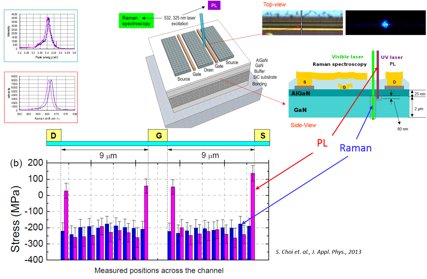
Micro-Raman spectroscopy and photoluminescence can be used for mechanical stress measurement (<0.5 µm lateral resolution) with a variable probing depth.
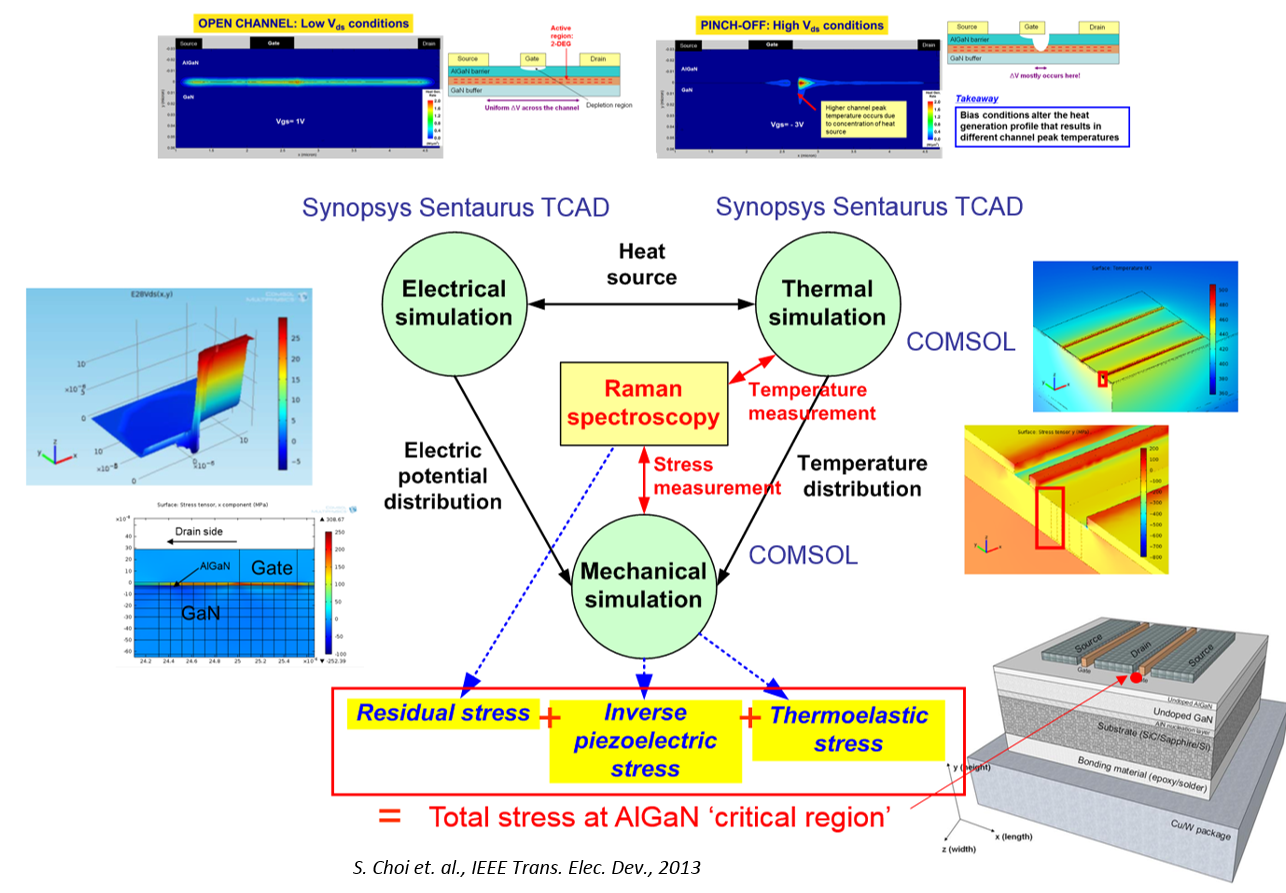
Multi-physics based simulation is performed to link, for instance, semiconductor device physics with the converse piezoelectric effect and heat transfer. Simulations are performed both at the device- and chip-levels.
Updated 9/26/2024


